
Over the past 15 years, the complexity of semiconductor chips has accelerated, with ASML (the world’s leading semiconductor machinery manufacturer) estimating that over 1.15 trillion semiconductor units were produced in 2021 [1].
The purpose of this report is to provide a detailed overview of the semiconductor supply chain to help investors better understand the different segments and components that go into making a chip. Additionally, we would like to use this as an opportunity to demonstrate how and where Carrara Capital are investing to take advantage of this attractive opportunity.
Semiconductor Materials
Semiconductor chips (or ‘microchips’) are the brains of electronic devices, primarily designed by familiar large US technology companies such as NVIDIA, Apple, Tesla, and Intel. They are tiny silicon wafers, housing millions of transistors, that can process (logic chips) and store (memory chips) information. These transistors act as miniature electronic switches, turning currents on and off as required to perform the operation.
A key aspect of the technology is the use of silicon in these wafers. Though in its pure form it does not conduct an electrical current, (a necessary feature for this application in circuit) silicon can be mixed with other materials (such as Boron or Phosphorous), making it a ‘semiconductor’. Silicon’s relative abundance and low cost of extraction compared to metals like copper make it a uniquely ideal material for use in chip manufacturing.
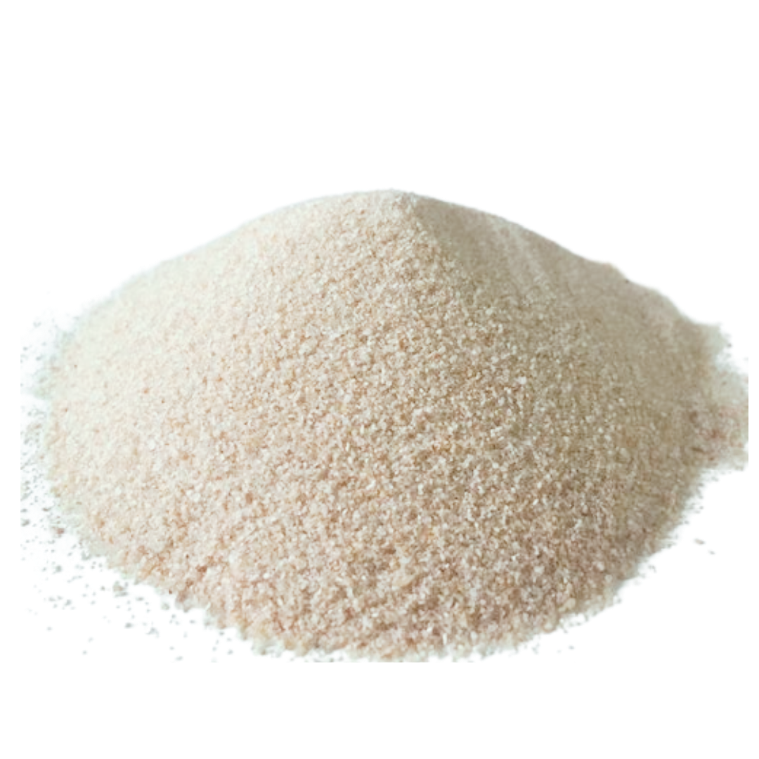
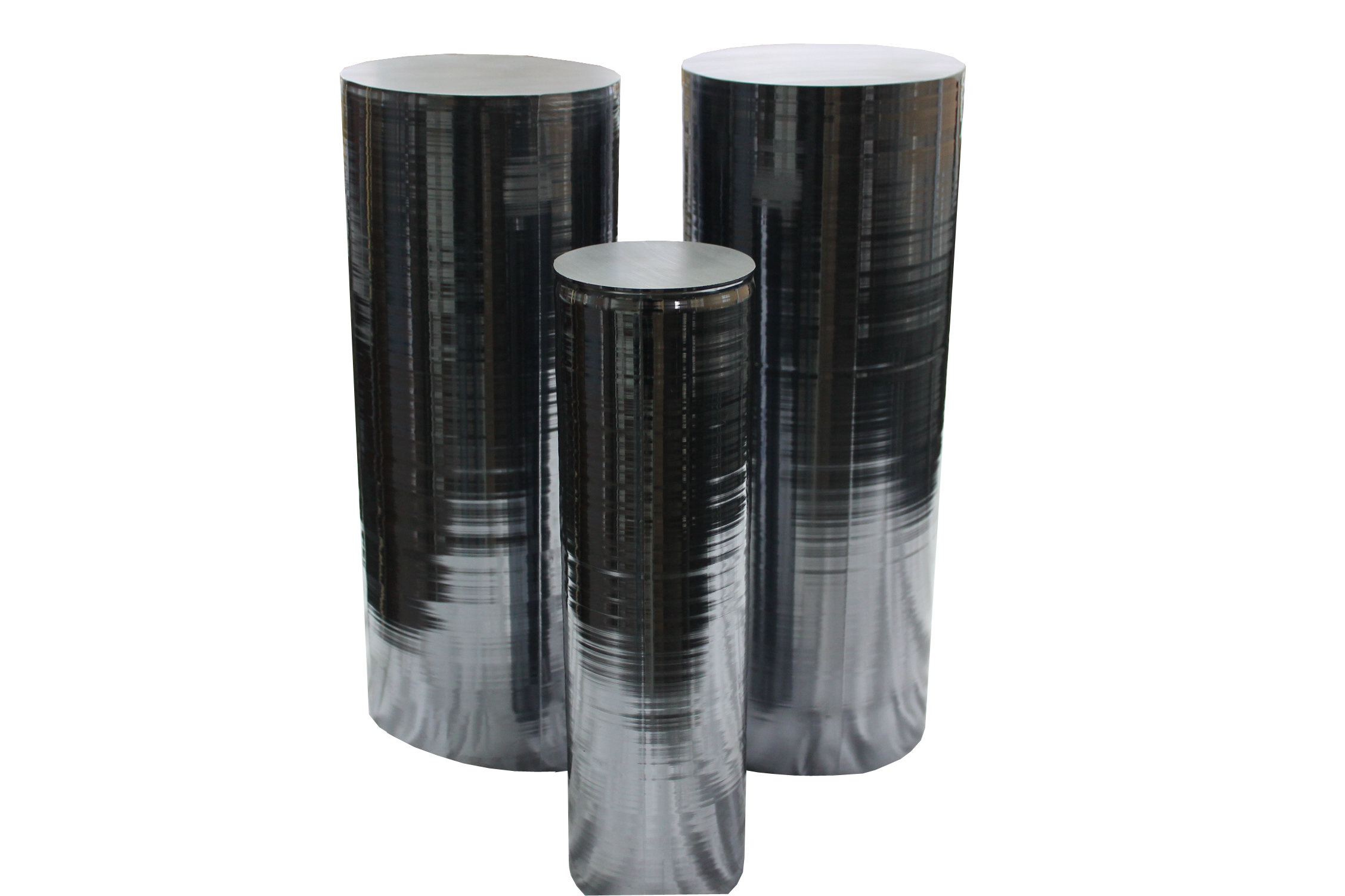
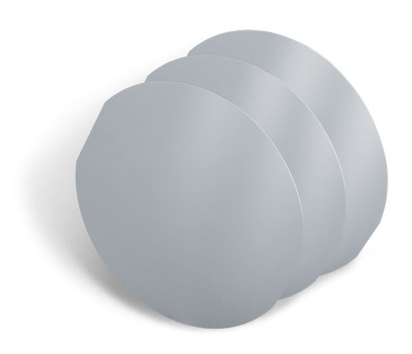
Silicon wafers are made from silica sand [2] which is melted at 1,420oC and cast into large cylinders called “ingots” [3]. They are then sliced to form silicon blank wafers [4] These stages are shown in the 3 images below.
Silicon blank wafers are created in highly specialised foundries with each individual large-scale semiconductor manufacturing foundry costing over US$15bn to setup [5]. In Q1 2023, Taiwan’s TSMC holds 60% global market share, followed by Samsung (Korea,13%), Global Foundries (US, 7%) and UMC (Taiwan, 7%) [6]
The Semiconductor Manufacturing Process
There are six specific steps involved in the semiconductor manufacturing process [7];
Deposition – The wafer blank is polished before thin films of conducting, isolating, and semiconducting material are deposited on it to enable the first “layer” to be printed on it.
Photoresist Coating – The wafer is then covered with a light-sensitive coating called a “photoresist”. There are 2 types of photoresists: positive and negative. The difference between each type is the chemical structure of the material and the way they react to light. With positive photoresist, the areas exposed to ultraviolet light change their structure and are made more soluble – readying them for etching and deposition. With negative photoresist, areas hit by light become stronger and more resistant to dissolving.
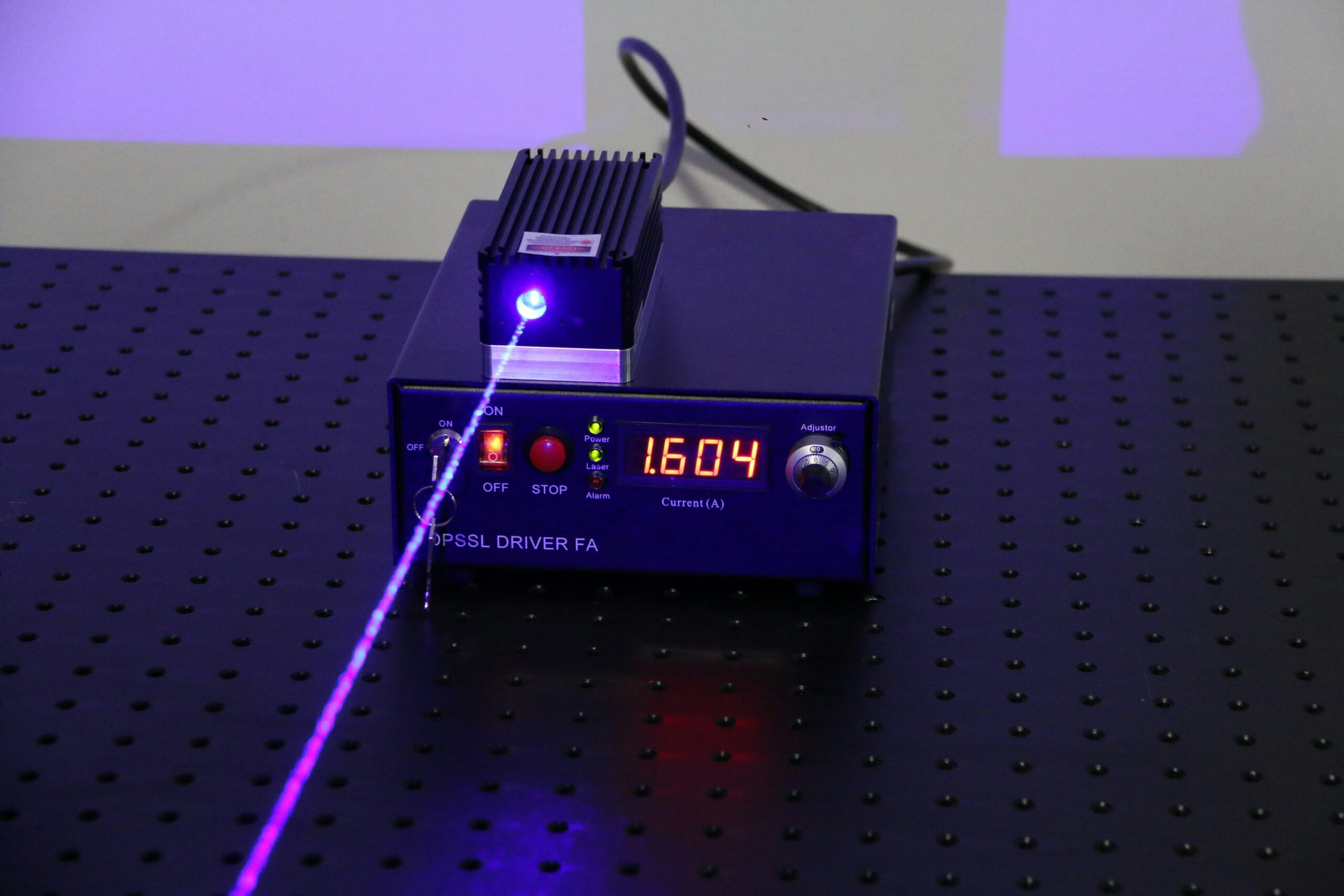
Lithography – The wafer is next exposed to ultraviolet light (either deep or extreme) through a lithography machine. The leading manufacturer of these machines is ASML. The light causes a chemical change in the wafer, whereby the positive photoresist areas are dissolved (outlined above) and the negative photoresist areas are strengthened.
Etch – The wafer is then baked, which washes away the dissolved sections created in the lithography process, leaving behind a nanometre-scale 3D structure of open channels and walls.
Microchips are made up of hundreds of individual layers, with the process of lithography and etching repeated over a period that can take up to 3 months.
Ion implantation – Sputtering machinery creates a gaseous plasma that bombard the wafer with a thin film of positive and negative ions that tune the electrical conducting properties of each channel in the semiconductor to form individual nanoscale transistors in each channel.
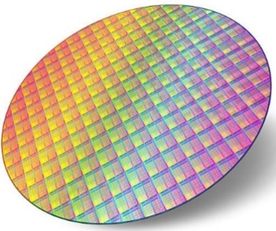
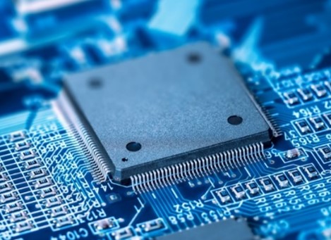
Packaging – The last step is packaging, which begins by slicing the 200-300mm semiconductor wafer, shown in the left image below [8], into individual chips. Each chip is then placed onto a substrate, which use metal foils to direct the input and output electrical signals from the microchip to other parts of the electronic device. These can be seen in the right image below [9].
Semiconductor Manufacturing Equipment
The miniaturisation of semiconductors has occurred through the development of increasingly complex semiconductor manufacturing equipment. Global sales of semiconductor equipment were estimated at US$126bn in 2023 [10], but rising demand from AI, IoT, EV’s and other new technology platforms is expected to see capital expenditure on semiconductor equipment and associated tools used in the manufacturing process grow to US$174bn by 2030 [11].
Equipment sales in 2023 were primarily targeted at silicon wafer production (90% of sales), which are used to make logic and memory chips, while testing equipment (6%) and assembly/packaging (4%) made up the balance of sales.
The estimated market size of each individual equipment type, and the world’s leading semiconductor machinery makers include:
Lithography machines – The lithography machine market had estimated global sales of US$27bn in 2023 [12]. ASML dominates the market with 83% market share, followed by Japan’s Nikon Corporation (10%) and Canon (7%).
Deposition Tools – The global deposition equipment market was estimated at US$17bn in 2023 [13]. Leading players include Applied Materials (AMAT), ASML, and Lam Research.
Dry etchers – The dry etching semiconductor market was estimated at US$24bn in 2023 [14]. Leading etching equipment makers include Applied Materials, Hitachi, Lam Research and Tokyo Electron.
Sputtering Systems – The global market for sputtering systems was estimated at US$1.4bn in 2023 [15]. Leading equipment manufacturers include Japan’s Ulvac and Canon, Vapor Technologies, and Semicore Equipment.
Dicing machines – The global dicing machinery market was estimated at US$1.7bn in 2023[16]. Leading dicing equipment makers include KLA Tencor, China’s Suzhou Delphi Laser, and NXP Semiconductor.
X-ray alignment masks – The X-ray alignment mask market for semiconductor manufacturing was estimated at US$1.5bn in 2021 [17]. Leading equipment makers include Applied Materials, ASML, Canon and Nikon.
Semiconductor Chemicals
The semiconductor industry uses various chemical materials in the production of microchips. These materials are typically used in the manufacturing process and do not remain in the final product. The global market size of for electronic “wet” chemicals was estimated at US$3.8bn in 2023 and is forecast to reach US$8.4bn by 2028. [18]
Semiconductor process chemicals can be generally categorized as follows [19]:
Aqueous solutions – these include acids and bases that are used in the chemical etching process or clean the surface of the wafer during the manufacturing process. Examples include hydrochloric acid, sulfuric acid, ammonium hydroxide, tetramethylammonium hydroxide, ammonium fluoride and hydrofluoric acid.
Specialty gases – these are typically used in relatively small quantities as precursors to deliver a substance such as arsenic or tungsten onto the wafer or into the silicon lattice. Other specialty gases dry-etch a pattern onto the surface of the wafer. Examples include silane, phosphine, tungsten hexafluoride, arsine, carbon monoxide, fluorocarbons, and nitrogen trifluoride.
Organic compounds – These are used in solvents that clean the wafer through various stages of the manufacturing and photolithography processes. Examples include isopropanol, propylene glycol ethers, acetone, and n-Methyl Pyrrolidone.
Metallic compounds – applied to the wafer in specific locations to create transistors or are used to plate wafers to provide electrical connections. Examples include copper sulphate, aluminium oxide, and titanium oxide.
The world’s leading suppliers of wet chemicals for the electronics semiconductor market include BASF, Honeywell Intl., Eastman Chemical, Solvay, Avantor, Fujifilm, Kanto Chemical, Merck KGaA and Resonac. [20]
Types of Semiconductor Chips:
Logic Chips
These are the brains of electronic devices; they process information provided by sensors and perform set tasks. “Logic” implies processing, in which either a fixed operation is performed, or a set of varied instructions is executed according to software embedded in the chip.
There are three types of logic chips; CPU’s (central processing units) which were the first chips designed in the 1960’s by IBM. As demand for specific functionality in chips appeared over the last 2 decades, GPU’s (Graphic Processing Units) that are designed for visual displays, and NPU’s (neural processing units), designed for machine learning applications, have gradually replaced CPU’s.
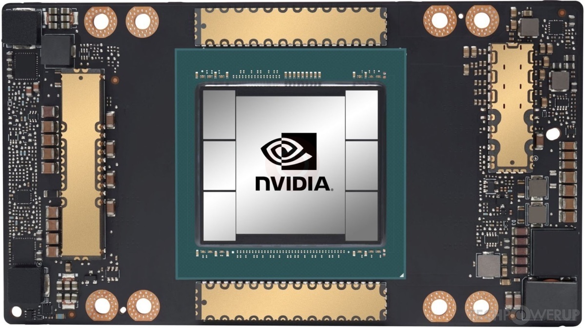
AI-enabled logic chips, including the NVIDIA A100 chip shown in the left image below [21], are used in just 6% of servers located in global data centres today. As demand for AI processing grows, providing improvements in operational productivity and intelligent decision making, the production of logic semiconductors will accelerate.
NVIDIA remains the dominant logic chip maker in the AI market, capturing an estimated 70% of AI chip sales in 2023. Priced at anywhere from US$16,000 to US$100,000, depending on volume order numbers and chip specifications, NVIDIA are believed to have an 18–24-month lead over its leading competitors.
Apple’s M1 Ultra logic chip, shown in the right image below [22], is another example of a logic chip which powers Apple’s suite of phones, laptops, tablets, and personal computers.
Tesla has been working on its own AI-chip (called the “Dojo”) that is designed specifically for training its autonomous driving models. Tesla is using the chip in its vast supercomputer that captures a constant stream of data from over five million vehicles for the past 3 years. It went into mass production in July 2023.
Silicon on Carbide Logic Chips
In the transition from ICE (Internal Combustion Engine) to Electric / Hybrid Vehicles, a shift from silicon wafer chips to Silicon Carbide (SiC) chips is needed to manage the significant jump in both voltage and current needed to both operate and electrically charge EVs. This is due to the increased hardness of SiC chips versus standard Silicon chips, which allow the semiconductor gate to remain open and for the electrical current to pass through the chip.
This presents an enormous long-term opportunity, with annual EV demand expected to grow to sixty-four million units per year in 2030 [23]. The SiC chip market is forecast to grow from US$2bn in 2022 to a range of US$11-14bn in 2030, presenting a strong opportunity for Infineon and ST Microelectronics, who commanded a combined global market share of 54% in 2022. [24]
Memory Chip Storage
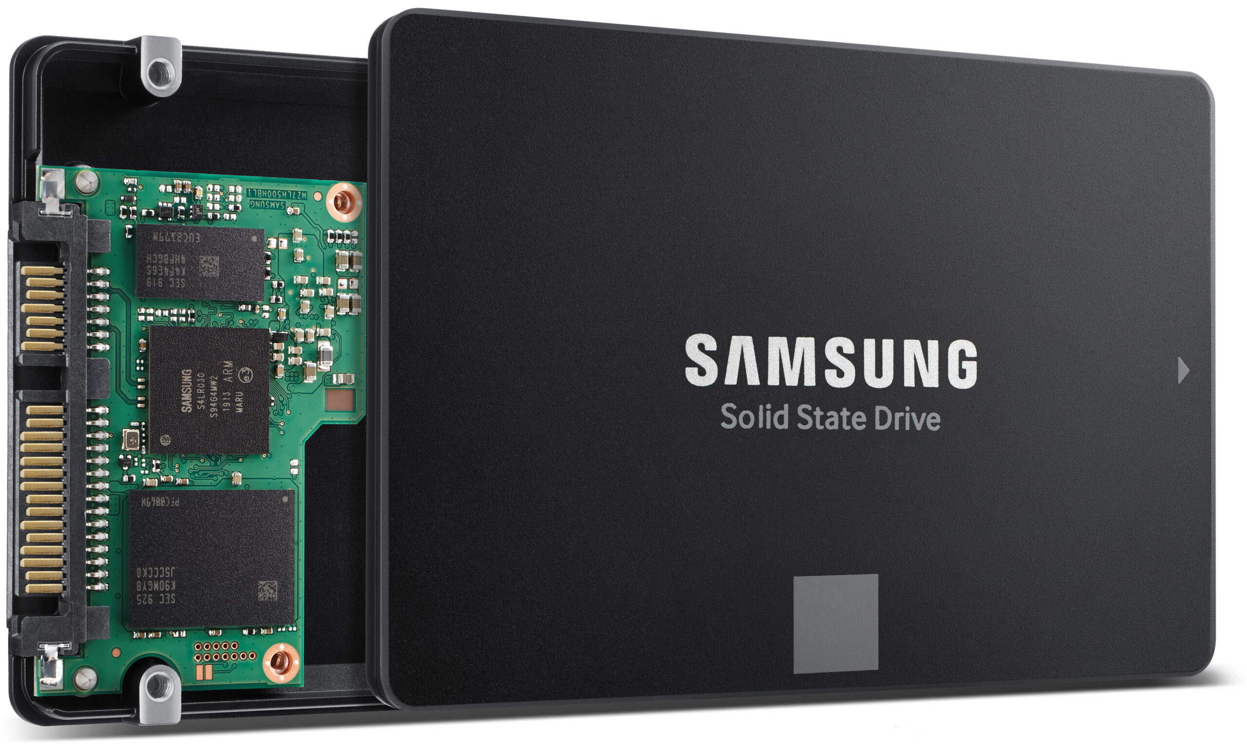
Memory chips store information in binary form (0 or 1). Solid State Drive (SSD) memory chips have billions of ‘cells’, which contain a capacitor (which store data as a charge) and a transistor (which activate the data). The transistor either charges or does not charge the capacitor, corresponding to one of two possible data units (‘1’ or ‘0’), which are the smallest units of data called a ‘bit’. A combination of eight bits (either 0’s or 1’s) is termed a ‘byte’, which represent a single letter or number depending on this combination. [25]
Hard Disc Drives (HDD’s) on the other hand use magnetic discs or platters to store data. The disc spins rapidly while an arm with read and write heads moves across them, reading and writing data to the disc. The head writes binary data in the form of ‘0’s’ and ‘1’s’ as tiny areas of magnetic north or south on the platter. A modern HDD can store over one trillion ‘0’ and ‘1’ bits on a single platter [26].
Types of Memory Chips
There are two specific types of memory chips, volatile and non-volatile. Volatile memory chips such as DRAM (Direct-Random-Access-Memory), shown in the left image below [27]. They are the most common technology used for a device’s main memory, because of their ability to quickly read and write data in each cell, but only work when the device is turned on.
Non-volatile chips such as NAND Flash chips, shown in the right image below [28], are responsible for the storage of data when an electronic device is switched off. [29]
Global sales of DRAM chips were estimated at US$97bn in 2023 and is forecast to reach US$127bn by 2031 [30]. Samsung Electronics was the world’s largest DRAM manufacturer in Q3 2023 with 39%, closed followed by Korean rival SK Hynix which held 34%. The other major manufacturer was US-based Micron Technologies with 23% share [31].
Global sales of NAND Flash memory chips were estimated at US$62bn in 2023 and are forecast to reach US$160bn in 2032 [32]. Like with DRAM chips, Samsung Electronics held the largest market share in Flash chip sales in Q2 2023 with 31%, followed by SK Hynix with 20% share. Three other companies made up the bulk of the remaining sales, Western Digital Corporation (17%), Kioxia (15%) and Micron (13%).
US Private Equity firm Bain Capital led an investment consortium which included SK Hynix, Apple, Dell Computers and Seagate Technologies to acquire Japan’s Kioxia in 2018 for US$18bn. Merger talks between Kioxia and Western Digital were blocked by SK Hynix in October 2023, through its 15% equity stake in Kioxia, over concerns it would leapfrog the combined entity into the #1 position in NAND Flash [33]. Recent rumours suggest merger talks may re-commence in April 2024 [34].
The NAND Flash market has struggled with production overcapacity issues and high inventory levels over the past 2 years, resulting in a 40% decline in unit prices for the larger 128GB chips and resulting in operating losses for Flash manufacturers [35]. A 50% reduction in production output, led by Samsung Electronics in 2023 and 2024 is expected to increase unit prices by 50% over H2 2024 / H1 2025 and allow a return to profitability [36].
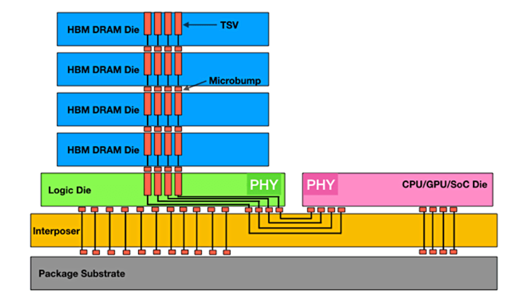
High Bandwith Memory
The highest growth opportunity in the semiconductor memory chip market over the next 5 years will be driven by the introduction of a new type of high-bandwidth memory (HBM3) chips that entered mass production at Samsung Electronics, SK Hynix, and Micron in Q2 2024. The HBM3 market is dominated by 2 Korean manufacturers, Samsung Electronics and SK Hynix, who have a combined market share approaching 95% [37]. NVIDIA announced on 20th March 2024 that they will source HBM3 chips from Samsung Electronics.
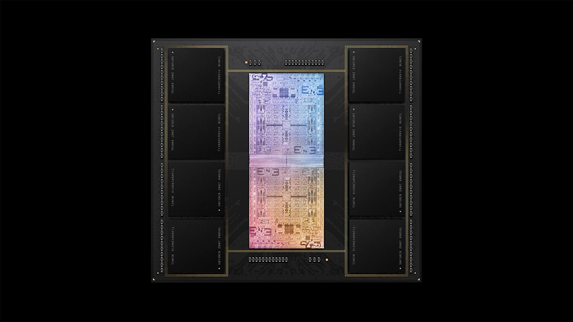
HBM chips are a type of memory interface used in 3-D stacked DRAM chips, which in turn are used in GPU chips, as well as servers and high-performance computers. By stacking multiple DRAM chips, as shown in the image below [38], the approach offers much higher bandwidth (data transfer speeds) and lower power consumption than traditional DRAM chips. The technology allows up to 8 DRAM chips to be stacked on top of each other, shortening the distance that data must travel between the memory and logic chip interface [39]. This approach allows AI computer chips to operate faster, with substantially lower power usage.
Carrara Capital’s current investments in the semiconductor supply chain
We believe this thematic is in its early infancy and offers a long-term (3-5 years+) investment opportunity from accelerating demand from AI, IoT, Electric vehicles, and personal electronic devices, amongst many other drivers. Each of these companies is amongst the top three global leaders in their sub-segment of the semiconductor chain, with some companies dominating across multiple sub-sectors.
We currently have investments in the following areas of the semiconductor supply chain:
Foundry Manufacturing – Taiwan Semiconductor (TSMC)
High Bandwidth Memory Chips – Samsung Electronics, SK Hynix
Silicon on Carbide Chips – Infineon, ST Microelectronics
Semiconductor Chemicals – Merck KGaA
Snapshot: Fundamentals
Company | Country | 2024 EV/EBITDA (x) | 2025 EV/EBITDA (x) | FY24-26 EPS CAGR (%) |
|---|---|---|---|---|
TSMC | Taiwan | 10.4 | 8.3 | 21% |
Samsung Electronics | Korea | 4.1 | 3.2 | 26% |
SK Hynix | Korea | 4.7 | 3.4 | 40% |
Infineon | Germany | 8.1 | 6.4 | 21% |
ST Microelectronics | France | 6.2 | 4.8 | 23% |
Merck KGaA | Germany | 10.3 | 9.3 | 11% |
Resonac | Japan | 8.2 | 6.4 | 73% |
Comparisons
Company | Country | 2024 EV/EBITDA (x) | 2025 EV/EBITDA (x) | FY24-26 EPS CAGR (%) |
|---|---|---|---|---|
NVIDIA | USA | 37.0 | 31.0 | 57% |
ASML | The Netherlands | 36.8 | 24.8 | 18% |
We are excited to watch the sector develop and are building on our existing research with a view to expand our holdings in the coming months, focusing on leading companies with attractively priced access to this significant growth opportunity.
Conclusion
The sheer complexity of the technology and the speed at which the sector is growing makes investing in the underlying supply chain without meticulous due diligence a coin toss at best. We believe in setting aside noisy headlines for specialist research and fundamental data, allowing us to diversify across companies and geographies to avoid concentration risk and to seek out value. In a sector which has rallied strongly over the past 12 months, we see significant potential upside and think focusing on the supply chain as a whole is a more rational approach instead of betting on single race winners.
Citations & Footnotes
[1] https://www.asml.com/en/technology/all-about-microchips/microchip-basics
[2] https://www.istockphoto.com/photos/silica-sand
[3] https://www.universitywafer.com/Silicon_Ingot/silicon_ingot.html
[4], [5] https://www.asml.com/en/technology/all-about-microchips/how-microchips-are-made
[6] https://www.visualcapitalist.com/semiconductor-foundry-companies-ranked/
[8] https://www.istockphoto.com/photos/wafer
[10] https://www.meticulousresearch.com/product/semiconductor-manufacturing-equipment-market-5432
[12] https://www.researchandmarkets.com/reports/5239464/semiconductor-lithography-equipment-market
[13] https://www.mordorintelligence.com/industry-reports/semiconductor-cvd-equipment-market
[14] https://www.mordorintelligence.com/industry-reports/semiconductor-etch-equipment-market
[15] https://www.360iresearch.com/library/intelligence/sputtering-equipment
[16] https://www.htfmarketintelligence.com/report/global-dicing-equipment-market
[17] https://www.verifiedmarketresearch.com/product/mask-alignment-systems-market/
[18] https://www.marketsandmarkets.com/Market-Reports/electronic-wet-chemical-market-265979069.html
[21] https://www.cnbc.com/2023/02/23/nvidias-a100-is-the-10000-chip-powering-the-race-for-ai-.html
[24] https://evertiq.com/news/55022
[25] https://semiengineering.com/whats-really-happening-inside-memory/
[26] https://cs.stanford.edu/people/nick/how-hard-drive-works/
[27] https://www.ahmedabadmirror.com/worlds-fastest-graphics-dram-chip-finally-here/81839049.html
[28]https://cdn.ttgtmedia.com/rms/onlineImages/samsung_v6ssd_half_column_mobile.jpg
[29] https://www.asml.com/en/technology/all-about-microchips/microchip-basics
[31] https://www.statista.com/statistics/271726/global-market-share-held-by-dram-chip-vendors-since-2010/
[32] https://www.expertmarketresearch.com/reports/nand-flash-memory-market
[35] https://www.flashbay.com.au/support/faq/NAND-flash
[38] https://www.theregister.com/2021/10/20/sk_hynix_hbm3/
[39] https://www.tomshardware.com/reviews/glossary-hbm-hbm2-high-bandwidth-memory-definition,5889.html


